WORLD LEADER IN POLARIZATION MEASUREMENT INSTRUMENTATION
1971-2021 Celebrating 50+ Years

![]()
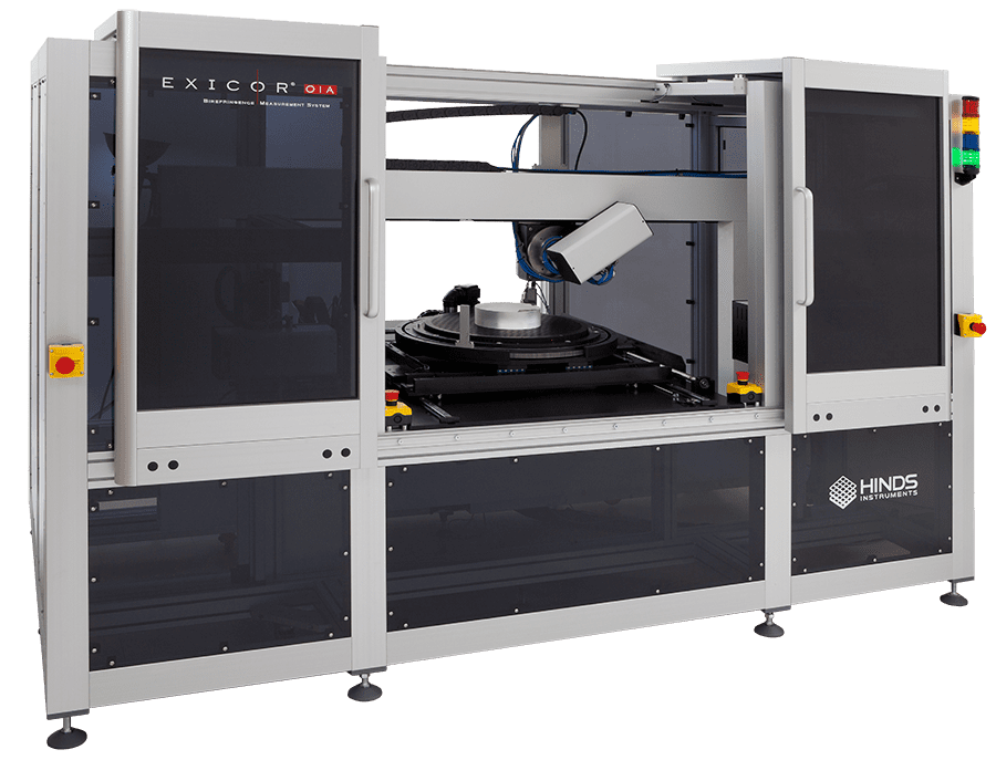
Our Polarization Measurement Systems & Components
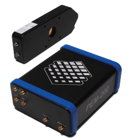
Components
The foundation of our most powerful systems. Also used extensively in laboratory and research settings.
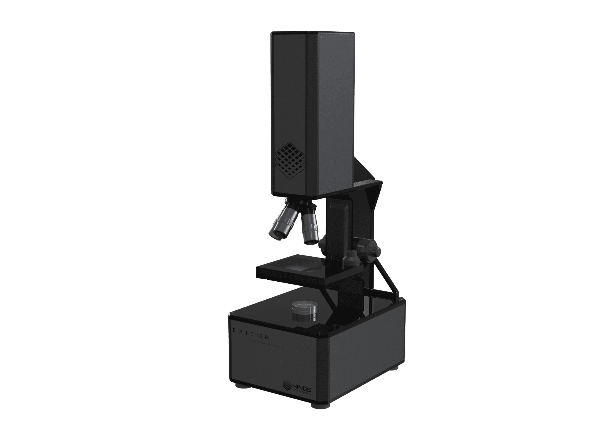
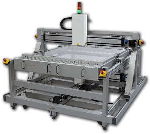
The Exicor® MicroImager™
The Exicor MicroImager is ideal for measuring birefringence in biological structures, glass, crystals, and many other organic and inorganic samples.
View DetailsFeatured Article
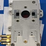
JPL and Hinds Instruments: Celebrating Nearly Two Decades of Collaborative Design to Put PEMs in Space Under NASA Projects
JPL and Hinds Instruments team up to put PEMS in space under NASA projects.
Upcoming Event


We’re Creating a Path to a Better Measured Future
Hinds Instruments has been solving complex problems in polarization metrology for more than 50 years. Our award-winning birefringence measurement systems, polarimeters, and electro-optical components allow you to perform the research and advanced quality control you need with complete confidence.