Stress in Silicon
The growth of single crystal silicon boules is at the heart of the photolithography process. The quality of wafers made from slicing the boules is fundamental to the quality of devices made from them in both the microelectronics and solar industries. Stress in the boules is an indicator of low quality for the manufacturing processes that follow. It is expensive to build up an entire circuit or solar cell only to find late in the process that the starting material was flawed. Historically, however, there was not a good method to determine the stress in the silicon boule early in the process.
Recently, Hinds Instruments, in conjunction with SolarWorld, has developed a near infrared Exicor® birefringence measurement system capable of determining stress in silicon ingots BEFORE they are sliced into wafers. In a study done by Dr. Wang of Hinds and Dr. Seipel of Solar World, high birefringence measurements in the ingot were linked to flaws in wafers cut from those regions.
The near IR Exicor system is capable of supporting an ingot and can transmit a measurement beam through an 8″ diameter ingot.
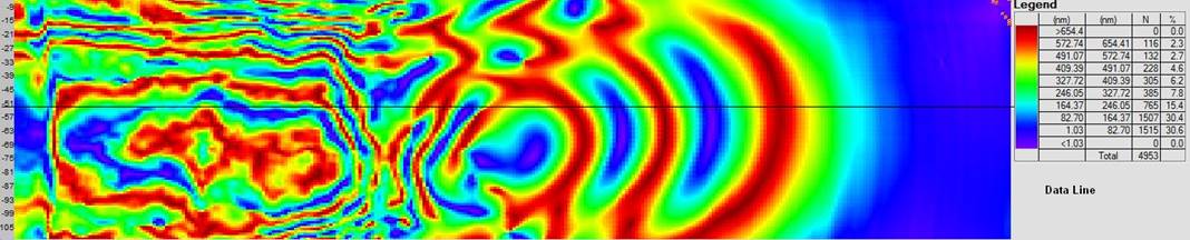
Figure: Exicor scan of a silicon ingot.
SUGGESTED PRODUCTS:
Contact us for more information about our near infrared Exicor birefringence measurement system.