Solar Cell Birefringence
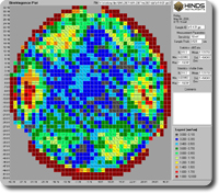
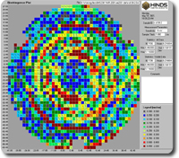
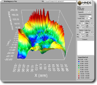
Solar cell (solar panel) birefringence is caused by stress in the silicon manufacturing process. This stress has been linked to lowered lifetimes in photovoltaic applications1 and low manufacturing yields. Hinds Instruments Exicor® NIR is capable of plotting these stresses in two dimensions in silicon wafers.
Left: Residual birefringence map of sample A (diameter: 90 mm and thickness: 5.25 mm); Center: Residual birefringence map of a 4” silicon wafer; Right: Residual birefringence map of sample B (diameter 65 mm x 65 mm x 10 mm)
Silicon Ingot Birefringence
Residual stress birefringence in the bulk ingots can be identified using the Exicor NIR system. Through process evaluation, this measurement can help identify problem material before it is processed, improving sawing yield and minimizing the investment in potentially problematic materials.
Above: Residual birefringence map of a silicon ingot showing low birefringence on the right end.
SYSTEMS AVAILABLE:
FURTHER READING
Contact us to see how Hinds Instruments works with our customers to solve complex metrology problems.


